If you’ve ever sent a Gerber file to a prototype PCB assembly shop only to get back a board that either doesn’t work, has weird connectivity issues, or costs way more than you expected, you know how frustrating a little misstep in layout can be. I’ve been running a prototype PCB assembly business for 12 years, and I’ve seen it all: designers cutting corners on spacing for a tiny 0402 resistor, forgetting to leave room for a test point, or placing a high-frequency crystal right next to a noisy microcontroller. Prototype builds aren’t like mass production runs—there’s no room for extra re-spins, because prototype schedules are tight, budgets are thin, and you’re often racing to test a new product before your competition. Over the years, I’ve refined a list of non-negotiable layout considerations specifically for prototypes, because the rules for a 10,000-unit run just don’t apply when you’re building 5 or 10 boards to test a concept. Prototype PCB Assembly

First up, test points. I can’t tell you how many times a designer has skipped test points to save space, only to have our assembly team call us a week later asking how to debug the board. For prototypes, test points aren’t a “nice to have”—they’re how you troubleshoot when your LED won’t turn on, or your sensor isn’t reading data. The rule of thumb here is simple: every net that’s critical to your design needs a test point. That means power rails, ground, clock signals, and any I/O line that connects to a connector or external component. But it’s not just about placing a test point. Prototypes often use manual probing rather than automated test equipment (ATE), so test points need to be big enough—at least 0.02 inches in diameter, with a clearance of 0.01 inches around them. If you’re working with fine-pitch components, like a 0.5mm pitch QFP, you can’t always fit a test point on every pin, but leave at least one test point per voltage domain and one per major signal group. Also, make sure test points aren’t placed under components or where they’ll be covered by solder mask openings for other pads. We see this all the time: a test point is right next to a fine-pitch IC, and when we assemble the board, the solder mask bridges the test point to a signal pin, killing that net. It sounds small, but it adds hours of rework and delays your prototype.
Next, component placement. Mass production layout might prioritize packing as many parts as possible to save material cost, but prototypes are the opposite. You need to place components with debug and rework in mind. Start by separating high-speed, high-frequency components from low-speed analog and digital parts. A 10MHz clock oscillator placed next to a temperature sensor, for example, will cause enough noise to make your sensor readings inconsistent—something you’ll never catch in a simulation, and that could waste weeks of testing. For prototypes, give yourself at least 0.1 inches of space between components that have a 10MHz or higher clock, or between analog signal paths and digital switching nodes. Also, leave a 0.2-inch margin around the edge of the board for mounting holes and standoffs. Prototypes often get bolted to test fixtures or enclosures, and if a component is too close to the edge, it’ll be damaged when you tighten the screws. Even better: place large, easy-to-hold components, like connectors and voltage regulators, along the edges of the board. That way, when you’re testing, you don’t have to reach under a bulky microcontroller to plug in a cable or swap a regulator. I remember one client last year who designed a wearable prototype with the USB connector tucked right next to the main microcontroller. When they tried to plug in a test cable, they ripped off the connector pad, and we had to rework the whole board—costing them twice their original assembly fee and a week of their timeline. Don’t make that mistake.
Then there’s spacing and clearance. For mass production, you can sometimes get away with tighter spacing between traces, because ATE and automated solder paste printers can handle precision down to 0.005 inches. But prototypes are built with more manual steps, especially if you’re doing small batches of 5 to 10 boards, and solder bridges are way more common when spacing is too tight. For prototype layouts, keep at least 0.008 inches of clearance between all signal traces, and at least 0.01 inches between power and ground traces, even for low-voltage designs. If you’re working with high-voltage prototypes—say, a 12V or 24V power rail adjacent to a low-voltage microcontroller—step that up to 0.02 inches minimum. We’ve had clients send us boards with 0.005-inch clearance between a 5V rail and a 3.3V signal trace, and during assembly, a tiny amount of solder wicks over, shorting the two nets. Fixing that on a prototype takes hours of rework, because you can’t just spin a new board. Also, don’t forget clearance around drill holes. Prototype PCBs often use standard holes for mounting or through-hole components, and if a trace is too close to a drill hole, the drilling process can tear the trace, or create a short between two adjacent holes. Leave at least 0.01 inches between any trace and a drill hole’s center, and 0.02 inches for holes larger than 0.05 inches.
Power distribution is another big one for prototypes. In mass production, you might use a wide power plane or multiple thinner planes for different voltage domains, but for prototypes, power planes can cause more problems than they solve. When prototypes have issues, you need to be able to trace where a voltage drop or noise is coming from, and a solid power plane can hide that. Instead, use routed power rails for prototypes. Keep power rails as wide as possible to minimize voltage drop: for a 1A current draw, use a 0.02-inch wide trace; for 2A, go to 0.04 inches. Also, add a bulk capacitor near the main power input, and a 0.1µF decoupling capacitor within 0.1 inches of every power pin on your ICs. Prototype boards almost always have unstable power when the designer skips decoupling. I’ve seen a Bluetooth module work great on a test bench with a lab power supply, only to fail repeatedly when mounted on a prototype board because there was no decoupling capacitor. The board’s trace inductance was causing voltage spikes that crashed the module. It’s a cheap fix in layout, but if you miss it, you’ll waste weeks debugging hardware when the problem was simple. Also, label all power rails clearly in your silkscreen—we’ve had designers label a 3.3V rail as “3V” and a 5V rail as “5V,” leading us to assemble the wrong regulator, and that ruined a board. Silkscreen isn’t just for looks; it’s critical for prototype assembly and testing.
Thermal management is often overlooked in prototype layouts, especially for low-power designs. But if your prototype has a power-hungry component like a linear regulator or a motor driver, a hot IC can cause inconsistent performance or even burn out during testing. For prototypes, add thermal relief pads for any surface-mount power components, and leave exposed copper under them to help dissipate heat. If you’re expecting more than 1W of heat from a component, add a few vias between the exposed copper and the inner ground plane to carry the heat away. Just don’t overdo it with vias—too many vias under a power pad can weaken the solder joint during reflow, leading to a cold solder connection. I learned that lesson early: a client had a 2W linear regulator on their prototype, and they added 10 vias under the exposed pad. When we ran the reflow process, the vias pulled heat away from the pad, so the solder never fully melted, and the regulator fell off during testing. We cut back to 3 vias, and the issue was gone.
One final consideration that’s unique to prototypes: allow for easy modification. Most prototype designs aren’t final the first time around. You’ll want to swap a resistor value, adjust a trace, or move a component after your first test run. When laying out your prototype board, leave extra space around high-value components, like resistors, capacitors, and connectors, so you can cut or add traces if needed. Don’t route traces in tight, unchangeable paths. If you have a signal that might need adjustment later, leave a spare test point next to it, so you can attach a probe or even add a jumper wire if you need to modify the circuit. I recommend including at least one spare test point for every 10 nets on your board, because you’ll almost certainly need it when you’re debugging the first prototype. I once worked with a startup that was testing a sensor array, and after their first prototype, they realized they needed to swap two signals between the microcontroller and the sensor. Instead of waiting a week for a new board, they used jumper wires between our extra test points and the sensor pins, and they were able to get their data immediately. That flexibility is priceless in prototype work.
At the end of the day, prototype PCB layout is less about perfection and more about practicality. Mass production layouts are optimized for speed and cost in high volume, but prototype layouts are optimized for debug, flexibility, and reliability in small batches. If you get these considerations right—test points for debugging, generous spacing for component access, enough clearance to avoid solder bridges, clear power distribution with decoupling, basic thermal management, and extra room for modifications—your prototype will work the first time (or the second, at worst) without unnecessary delays or extra costs.
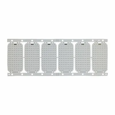
If you’re working on a new design and need help making sure your layout is ready for prototype assembly, our team has spent years helping designers avoid the common pitfalls that delay prototype schedules. We specialize in small-batch prototype builds, and we can review your layout before you send it to manufacturing to catch issues you might have missed. Contact us today to discuss your prototype assembly needs and get your board designed and built on time.
Flex PCB References
IPC-2221, Generic Standard on Printed Board Design, IPC Association Connecting Electronics Industries, 2022.
IPC-7351, Generic Requirements for Surface Mount Design and Land Pattern Standard, IPC Association Connecting Electronics Industries, 2021.
Huaswin Electronics Technology Co., Ltd.
Address: Building A2, Hao Hai Hong Industrial Park, No.3 Yu He Road, Gong He, Sha Jing, Bao An, Shenzhen
E-mail: sales@huaswin.com
WebSite: https://www.huaswin-pcba.com/
